Bias sensor
The bias sensors purpose is to detect any deviation from the nominal bias level without being influenced by the current
distribution over the output transistors, in other words, independently of the current delivered to the load (RL ). This is
accomplished by sensing the voltages across the source resistors of the output stage and passing them to a non-linear
network, comprising two current mirrors (transistor pairs T3,4 and T5,6 respectively). Two equal reference currents are supplied
to the inputs of the mirrors via R6 and R8 Since the voltage across each source resistor adds an offset to Vbe of T3 and T6,
the currents reflected by them will be lower than the reference.Under quiescent conditions, this offset is such that each mirror
reflects only 50% of the reference current. As dictated by the laws of physics, this condition is met if the offset voltage is 18mV
(at room temperature*). Together with R1 and R2 , this 18mV defines the quiescent current of the output stage (e.g. 100mA if
R1 = R2 =0.18 Ohm). To maintain this condition, the reflected currents are summed together and subtracted from a third
reference current supplied by R9. The resulting difference, IERR, tells us whether the output stage is under, correct or over
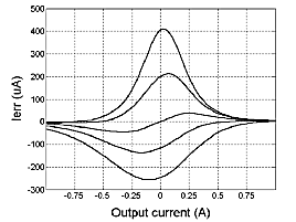
biased. This means, IERR can be used as a feedback signal, Fig. 2. Next, what happens in the presence of small or medium
signals? This is illustrated by the middle curve of Fig. 3. It shows the relationship between error signal and output current at the
nominal bias level. As one can see, the crux is that the error signal stays very close to zero. Apparently, the non-linear behavior
of the mosfets, in particular in their weak and moderate inversion region, matches the characteristics of the bias sensor quite
well. The other curves show the error signal if the output stage is forced to an under or over biased state. Beyond output
currents of ca. 0.6A the error signal is pinched off. This looks like a disadvantage, but it turned out to be beneficial, as
explained below. Finally, what happens in the presence of large signals? Suppose T1 carries a large current and T2 is turned
off. In this case the reflected current in T3 is zero, while in T6 it is 100%. Summed together and subtracted from the third
reference, the resultant error signal is again zero. This is exactly what we want, as an output stage operating in class-B
provides no information about the quiescent current, therefore, the error signal has been pinched off in order to preserve the
charge of the integrators capacitor (C3).
Since music has a high peak/average ratio - some 20dB - the average signal level - even at maximum volume - is well within
the capture range of the bias sensor. Sine waves at full power give no trouble either, as the relative time traversing the capture
region is long enough to let the control loop do its work. However, a large square wave pushes the output stage continuously in
class-B and no error signal is produced at all, leaving the integrator in an undefined state.
Isolator
To avoid any adverse interaction between common mode and differential signals at the gates (node A and B), an isolator has
to be inserted somewhere inside the servo current loop. Putting it between bias sensor and integrator greatly simplifies the
circuit, as the integrator can now simply use the bias voltage as supply.
Given the bipolar nature of the error signal, two opto-couplers (U1, U2 ) are needed, one for charging, the other for discharging
C3. They are specified for operating at low currents (<1mA). Apart from their primary task (isolation), they serve one more
purpose: masking the tiny deviations of the error signal, as can be seen at the middle curve of fig. 3. The reduced transfer ratio
at very low currents from which any opto-coupler suffers (see Fig. 4), meets this purpose nicely. R11 delivers the supply voltage
to U1, while being limited by LED D3 reducing Vce of T3 and T6 to approximately the same level as T4 and T5 and preventing
simultaneous conduction of U1 and U2.
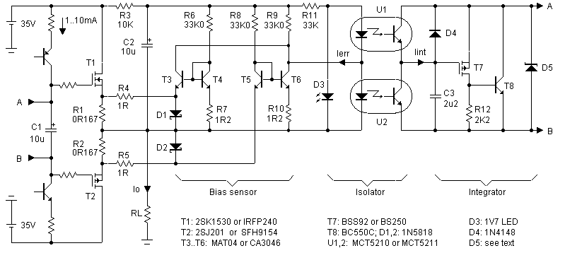
Integrator
Depending on the mosfets actually used, bias voltage can vary from 2 to 10V. To handle this range it leads almost automatically
to the kind of topology, as shown in fig. 1. In spite of its simplicity, this integrator, or to be more precise - integrating shunt
regulator, exhibits a dynamic output impedance that is low enough (<2 Ohm) to cope with AC currents from the driver stage. In
order to exclude interaction at AF, integrator capacitor C3 is rated such that the unity gain frequency of the servo loop falls
below the audio spectrum, somewhere between 1 and 10Hz, depending on transfer ratio of the opto-couplers. D4 discharges
C3 during switch off and protect the gate of T7. For reliable operation, low leakage at the integrator input is essential, so D4
should be protected from light. Zener diode D5 is rated at he maximum expected bias voltage plus a small margin and should
be adapted to fit a particular design. If some component fails or if nasty test signals have been applied, this diode protects the
output stage against excessive common mode currents.
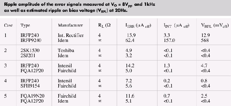
Accuracy
The bias level is very sensitive to mismatches of the transistor pairs and reference currents. Base-emitter voltages T3, T4, T5
and T6 respectively should match at least within 0.5mV. A quad transistor like a MAT04 or CA3086, selected on low Vos meets
this requirement. For the same reason, R6, R8 and R9 should match at least within 0.5% as well as the equivalent emitter
series resistors; hence R7 and R10 are rated slightly higher than R4 and R5. Since a MAT04 is equipped with small reverse
connected diodes between base and emitter, Schottky diodes D1, D2 are added to protect them.
Now we come to a moot point: the voltage of 18mV across R1 and R2 which all relies upon, varies linear with the absolute
ambient temperature*. Of course, it varies much less than the junction temperature of the output devices and thermal runaway is
precluded, but still it is not constant. It is not yet clear to me whether this should be regarded as flaw or feature, as one could
argue that the decreased transconductance of mosfets at elevated temperatures just needs an increased bias level.
Interestingly, a bias control IC from Linear Technology shows the same temperature dependence, which could not be explained
by an inherent shortcoming of the basic circuit. So I concluded that this property has been added on purpose. Asking why,
Linear Technology was unable to give a satisfactory explanation. If anybody could shed light on this matter, please let me know.
*Vbe = VT Ln2, where VT = kT/q, the thermal voltage (25.86mV at 300K).
Experimental results
To see if the circuit is generally applicable, I tested it on several combinations of mosfets, all capable of delivering 12 to 20A,
but of different types and brands. To minimise temperature effects, measurements were done at a reduced supply voltage of
2x16V, the mosfets mounted on a large heatsink with forced air cooling and at a frequency of 1kHz. Static measurements were
done at an even lower voltage, 2x7.5V. Since these were very time consuming, I have done this only in case 1 and 2.
In the first instance, dynamic behaviour of bias current was observed by means of an oscilloscope, but changes at various
output levels were hardly visible and difficult to quantify, except in case 1, which showed an increase of 5% at maximum output
power. Instead, I used a DVM to measure the ripple amplitude of the error signal before and after the isolator under load and no
load conditions. Next, I estimated the ripple on the bias voltage at 20Hz, according to VRPL = IINT / (2 * pi * f * C3 ), instead of a
direct measurement at 20Hz, because thermal modulation could be disturbing. See table for results.
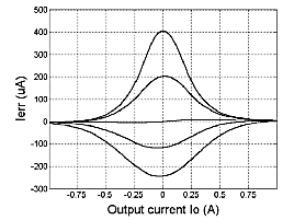
The first trial was rather disappointing, not to say confusing. The error-function, Fig. 5,is heavily skewed and ripple currents are
high (see table, case 1). Transconductances were reasonably matched - within 20%, so something else spoiled it. It appeared
that the output conductance (GOS) of the IRFP9240 was the culprit. At a drain current of 125 mA, GOS is about 5mA/V, while the
IRFP240 shows a GOS of only 0.4mA/V (corresponding to an Early voltage of 25V and 312V respectively). So an increase of
output voltage of 1V -without load- will increase the quiescent current by 4.6mA. No wonder that the error function is skewed. At
higher drain currents the IRFP9240 behaves better: at 1A for instance, the Early voltage raises to ca. 75V. This explains why
the ripple on IERR becomes much smaller when the output stage is loaded with low impedance. However, speaker impedances
are not always that low - at resonance up to tenfold, so a no load condition has also to be taken into account. Without blaming
the manufacturer, I cannot recommend this mosfet pair. After all, these devices were designed for switching, not for driveng
loudspeakers.
In the next trial I used a complementary pair from Toshiba, especially intended for linear applications: 2SK1530 and 2SJ201.
Due to closely matched transconductances (within 5%) and high Early voltage (over 300V) for both N- and P-channel parts, the
results were far better. The error function, Fig. 6, is in accordance with the simulation, although skew is slightly higher and in the
opposite direction. Ripple currents were hardly measurable.
In the last three cases I tested several other samples (courtesy of Fairchild) which are less expensive, but, as in case 1,
primarily targeted for fast switching. Results were almost as good as in case 2 and I see no reason not to use these mosfets,
except that the higher gate threshold voltage reduces the maximum output power somewhat, without using a boosted power
supply for the drivers.
I have also investigated a few combinations of two 20A N-channel and three 12A P-channel devices. Because no
improvements were seen, I will not discuss them any further. Using bjts instead of mosfets will probably not work at all, as Spice
simulations were very discouraging. For lack of Spice models, lateral d-mosfets have not been investigated.
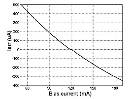
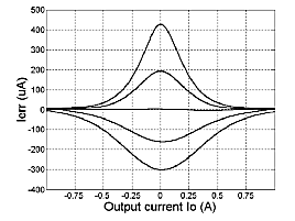
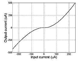
Fig. 2. Simulated error signal as function
of bias current (IREF =1mA, R1,2 = 0.167
Ohm , RL=inf. ).
Fig. 3 Simulated error signal as function
of output current at bias levels (from top
to bottom) of 60, 90, 120, 150 and
180mA. Notice that at 120mA this signal
stays close to zero.
Fig. 4. Transfer function of the opto-
isolator.
Conclusion
Provided that output devices are selected with some care, in particular with regard to trans- and output conductance, the
proposed circuit comes up to all expectations. Since the circuit acts only on the bias voltage and is not intrusive on any other
part of the amplifier, it should be easy to incorporate into new or existing designs like mentioned in ref. [8] and [9].
References
1. Finnegan, T, Going linear with power mosfets, part 2, EW, Sept. 1992, p.781.
2. Self, D, Thermal dynamics in audio power, EW, May 1996, pp. 410-415.
3. Roehr, W., The autobias amplifier, JAES, April 1982, pp. 208-216.
4. Siliconix, Mospower Application Handbook, Chapter 6, pp.105-110
5. Gevel, M. van de, Audio power with a new loop, EW, Feb. 1996, pp.140-143.
6. Datasheet LT1166, Automatic bias system, Linear Technology.
7. Brown, I., Opto-bias basis for better power amps, EW+WW, Feb. 1992, pp. 107-1098.
8. Hitachi Mosfet Handbook, Section 6.1, pp. 143-151
9. Stochino, G.,300V/µs power, EW, April 1997, pp.278-282
To download the original article in PDF format click here.
Fig. 5. Same as fig.
3, but measured on a
IRFP240/IRFP9240
pair at bias levels of
57, 85, 118, 142 and
171mA
Fig.6. Same as Fig.5,
but measured on a
2SK1530/2SJ201
pair.


Finished projects

Autobias for MOSFET audio output stages (published in Electronics World December 2003)
Its said that biasing vertical d-mosfets in a class-AB output stage is less critical than biasing their bipolar
counterparts. So many designers are content with the classical Vbe multiplier as bias generator. However, the
accuracy needed for utmost performance (in terms of cross-over distortion and quiescent dissipation), cannot be
provided by such a circuit, even when it is thermally coupled to one of the output devices.
Several factors may contribute to the lack of accuracy:
1) Mismatch between relative temperature coefficients of mosfets and bjts as consequence of the variability of the
gate threshold voltage as well as the temperature coefficient of Vgs
2) Thermal delay and attenuation of the coupling between output device and sensing element.
3) Drivers - if included - that operate at a different temperature.
4) Long-term drift of threshold voltages as a result of aging[1].
5) Errors in adjusting the bias level for each individual amplifier.
So it seems natural to replace the Vbe multiplier - which in fact provides a kind of error feed forward[2]- by a control
loop based on feedback of the bias current itself. In the past, several attempts have been undertaken in this
direction, but none of them seem to me suitable for high-end applications, as they are intrusive also on other parts
of the amplifier. This could raise distortion[3,4] , complicate HF compensation[5,6] or be incompatible[3,4,5] with a
complementary source follower arrangement (which I prefer), or could be too complex[7] . Nevertheless, reference
[5], ingenious in its own right, inspired me to a re-design that overcomes these shortcomings. The new design
comprises three sections: a bias urrent sensor, an isolator and an integrator. Each of them will be discussed below
in detail.